

This Is The Announcement Of New Enterprice 2020 Version Of Scientific Pre-seismic Electric Signal Data Acquisition System almost finished prototype, A Crisistech Labs Innovated Design. An Extremly Powerful, Small Device From Factor, Very Low Consuption Less Than 4.5W, Compact Design, Weight Less Than 1Kgr ,A High Grade Intergraded Accurate Measurement Device, Can Support 24/24hrs Pre-seismic Electrical Signal Recordings In Fully Customized Offsets, Variable Sampling Rate, Can Also Support Access Through Modern Telemetry Of The Recorded Data From Anywhere.
 WARNING THESE MODIFICATIONS ARE EXTREMLY DANGEROUS FOR PEOPLE WITH LOW EXPERIENCE TO SMPS HIGH VOLTAGE CIRCUITS. DO NOT ATTEMP THESE MODIFICATIONS IF YOU ARE NOT AN ELECTRONIC ENGINEER OR AUTHORIZED TECHNICIAN ELECTRICITY CAN HARM YOURSELF PERMANENTY, IT CAN CAUSE DISABILITY OR DEATH. I’M NOT RESPONSIBLE OR I HAVE NOTHING TO DO WITH YOUR ACTIONS. IF YOU DON’T UNDERSTAND PLEASE LEAVE THIS PAGE IMMEDIATELY. There Was An Emergency Task To Build A 12V 180A Power Supply But there was a deadline & I couldn’t Design It From The Beggining Spending Days & Weeks For A Single Lab Unit, So I decide To Use My Experience In SMPS Reverse Engineering. The First High Power SMPS I Was Found A HP PS3701-1 Spare Part Number 365063-001 From An Old ML350 Server Looks A Great Choise. The Reason Is Too Simple, All This Units Designed To Work In Parallel Mode Into HP Servers, So For Parallel Use I Had To Worried About The Lenght & The Diameter Of The Cabling Inside the Enclosure & Finally I Need To Use The Same Lenght Of Cables If I Had To Parallel More Than One Units.
  Specifications 1. Input 100-240VAC 2. Output Main Output +12V/60A, A Small Negative -12V/0.5a, & An Auxiliary Output +5V/1A First Of All I Had To Check My Memory About These PSU’s, Are Well Protected Against Short Circuit & Reverse Polarity? Yes!!! It Was Absolutely True. Each Of These Units Can Be Used In Series & Parallel Mode With A Few Modifications BUT NEVER TRY TO DO IT IF YOU ARE NOT A AUTHORIZED TECHNICIAN WITH EXPERIENCE TO HIGH POWER SMPS UNITS. There Was An Issue With The Negative Output Pole It Was Grounded & The Chassis Too But We’d Like A Grounded Chassis Anyway, So That Was Not Ideal For Serial Mode Use, It Could Be A Nightmare Trying Connect Two Units In Series Mode! I Had To Modify Each Unit Except The First One IN ANY CASE THIS ONE MUST BE GROUNDED So I Made A Decision To Teardown A Unit, But Before I Took A Few Measurements To Verify & Secure The Success Story…lol. As You Can See At The Photo There Are Four Outputs 12V At The Left & Right, But You Have To Split The Outputs Using 15 Amps Fuses To Avoid Possible Over Current Damage To Output Pads & Traces. All You Need To Know About Outputs Was Marked, See The Next Foto.
  I Had To Measure Each Output & To Take A Closer Look To The Whole PSU Design & Construction. I Noticed That The Green Status Light At The Back Side It Was Activated Only If I Had To Connect The Remote Control Switch Between The Pin RC & (-) Negative All Negative Outputs Are Located At The Left & Right Sides At The Edge You Can Connect It everywhere.
  Now I Had To Do A Careful Inspection About The Ground So I Had To Take A Closer Look At The Front Side Where Located The FAN & The Power Outputs. Aha!!! There Was An Issue There, The Enclosure Chassis Was In Contact With The Negative Outputs. I Had To Isolate This Area To Avoid A Connection Between Main Ground & Negative Output Pole For Each PSU Which Was The Second Or The Third In Series Of The Array. A Thin PVC Foil Placed With Silicon Glue To Isolate The Area As You Can See At The Next Foto
  After This I Had To Teardown The PSU To Continue The Mods! Take A Look After Removing The One Piece Of Enclosure.
 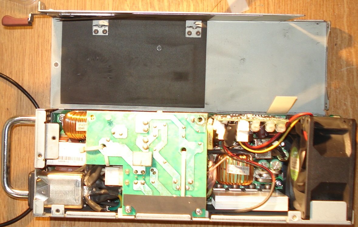 The First Thing I Had To Do Was To Remove The Ground Connection Between The Chassis & The Negative PCB Output Which Located Beside The Small Vertical Control Board. It Was Very Easy By Removing The Screw As Shown At The Next Foto
  Then I Had To Place A Small Foil Of PVC With Silicon Glue Between The Chassis Spacer & The PCB.
  DON’T PLACE THE SCREW BACK
  After This MOD I Had To Isolate The Main PSU Circuit From Earth Ground But I Had To Place A Capasitor Between Earth Ground & Main PSU Board For Ground Isolation & To Make A Path For AC Signals Between Ground & Main Board PCB. First Of All I Had To Move The Isolation Tube Sield From The Mains Plug Ground Pole. Then I Had To Remove The Yello Ground Cable From The Main’s Ground Pole
  Then I Had To Place A Capasitor Between The Cable & The Ground Pole. It Was Very Importand To Isolate Everything Included Capasitor & Cables After This Modification. A Capasitor Value of 100nf/275V AC X3 Series Or Greater Voltage It Will Be Fine.
 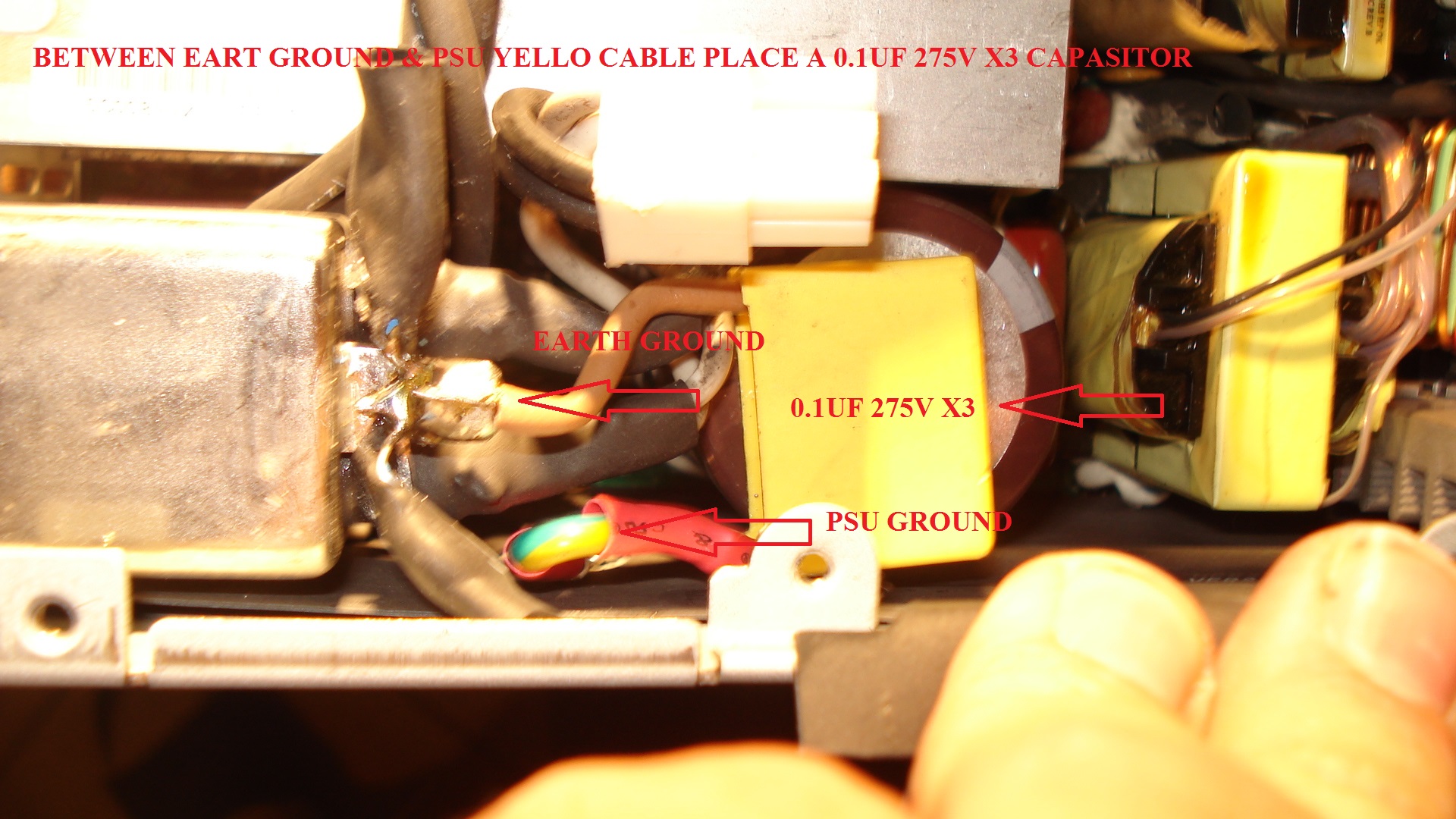 After All These Mods I Had To Close The Enclosure Back. PLEASE READ CARFEFULLY IT’S VERY IMPORTANT!!! I Had To Check About Any Unwanted Connections Between Chassis & Negative Outputs Before I Close The Enclosure. I Turn On The Switch Of The Non Grounded Second Unit & Between Ground & Negative Output Or Positive Pole Finally Was Measured At Least 110V AC!!! Next Step Was To Build An Automation Circuit & A Front Panel PCB To Protect Myself For Possible AC Leak Voltage At The Outputs When It Was In Use At The Bench. This Circuit Was An AC Signal Detector With Optical & Sound Alarm, I Think It’s Time To Explain It.
  I Had To Built 3 Of These PSU’s For Parallel & Series Use. As I Wrote Before The Second & Third Unit’s Was Floated Not Grounded So Any Possible Leak AC Voltage Can Harm Myself Or Any Connected DUT. I Had To Include A Protection Circuit For Myself & Other Users Safety, F.E. iF Someone Tries To Turn On The Second Ungrounded Unit & Working With It The Unit Will Be Floating & There It’s Quite Possible To Harm Himself Or DUT’s. So For Everyone Unsuspected Or layman Guy There Was A Back Door Directly To Death! This Issue Can Be Resolved With Warning Optical & Sound Alarm To Prevent The Possible Damage Or Failure In Case The Ground Was Missed Or Forgotten. My Suggestion Is To Read My Thoughts & Use This Device Wisely. When You Using These As Stand Alone Units. Don’t Touch The Output Or Connect A Device At The Second Or Third Unit Without Earth Ground Present At The Negative Pole Both Of These Units Please Take A Look At The Following Foto, Each Output Has It’s Own Thermal Fuse At 15A Each Unit Has 4 Outputs That Means 15mps x 4 = 60Amps. Each Unit Must Have The Same Leangh Of Cabling To Avoid Possible Port Over Load. Each Cable For Internal Cabling Is 8 AWG FOC (Free Oxygen Copper) Except The Main Negative Cable Which Is 4 AWG FOC Too.
 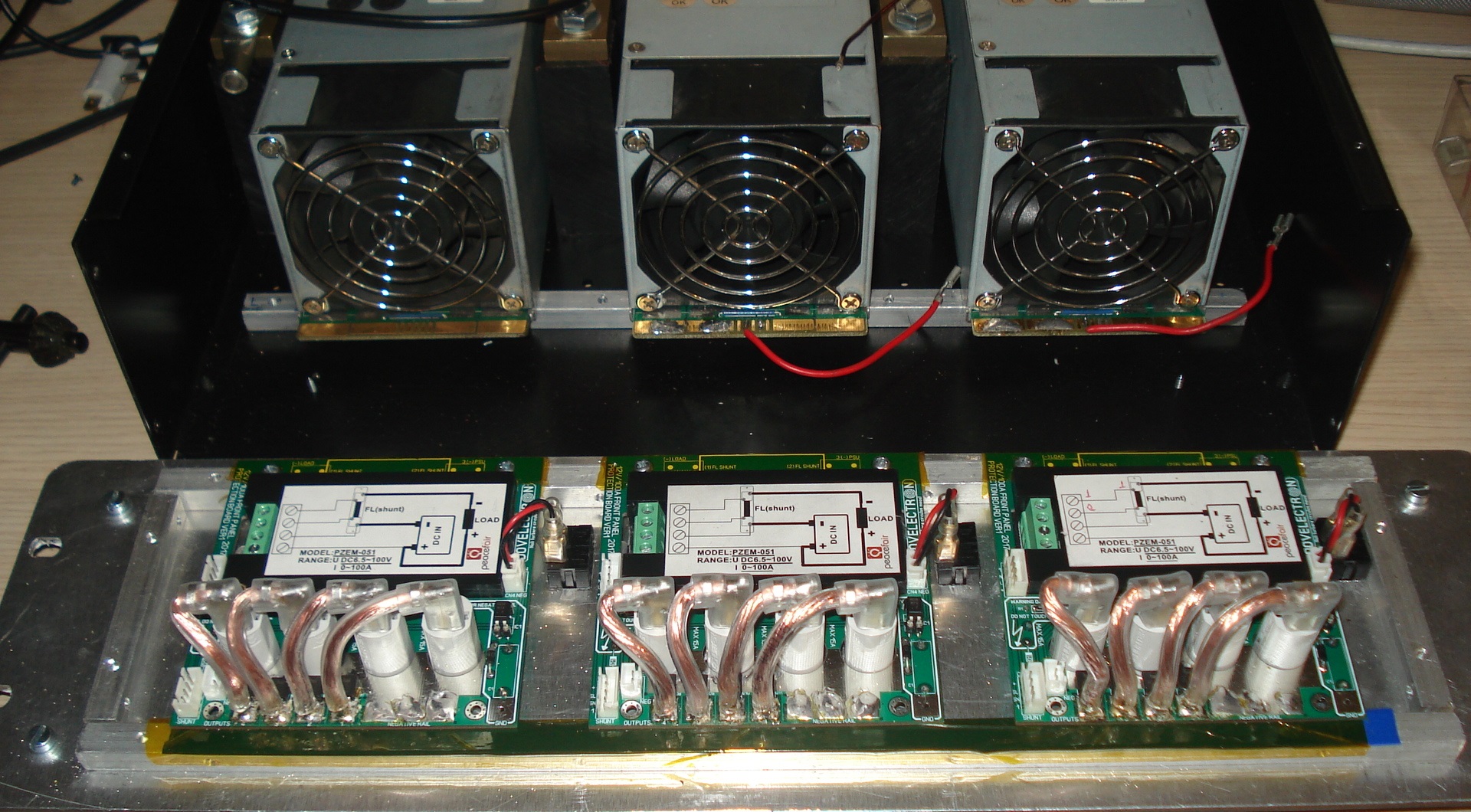 For This Project We Bought Cheap LCD Panel Meters For Voltage, Current, Power & Energy Data Logging. You Can See The Front Panel Inclunding Switches, Heavy Duty PCB Terminal Block Outputs, Panel Multi Meters, Thermal Resetable Fuses, Warning Sings Instructions & Functions. This Is The 40Amps Output Version Per Unit, The Latest One Was 60Amps Per Unit.
  Inside The Enclosure You Can See Three 100Amps Shunts One For Each PSU.
  Each Unit Has A Independent Input For Tha Main AC At The Back Side Panel.
  Suggested Connection Diagram Below There Was An Error Typing 108Amps In Parallel The Right Is 180Amps!
  Conclusions It’s Working Like A Charm! Alarms Are Working Pretty Well Too. We’ve Test It At 36V In Seies At 55Amps & It Was Perfect. We’ve Tested As 12V Stand Alone Each Unit But With Grounded For All Units The Common (-) Outputs 12V/55Amps. Finally The Great Test 12V/140Amps Rated To A Power Inverter! Kind Regards Akis T


This is a Front Panel board for most wanted RDVV PLL.


It can be used for all common versions from beggining until the 2006’s Versions.
The PCB design contains the following functions including a few older partitial designs i made many years ago for similar personal projects.
1. Analog Volume Control
2. Analog Power Control
3. RDVV LCD Main Display attached
4. Audio Peak Detector with Led
5. Analog Audio Level Meter (1991)
6. Analog PWR/SWR Meter (Only the panel meter session with the level controll but without PWR/SWR Coupler) (1987)
7. Thermal Protection for the RDVV Power Stage & For A Possible Linear Amplifier as a next power stage. (1983)
8. Tone Test Generator 1Khz (1981)
9. Mono MPX AF Input Selector.
10. Premphasis 50/75us Included + Input Selector. (1981)
11. SWR & Thermal Protection with optical & sound alarm. (1987)
Schematics, Gerbers And BOM List Are Available
This project is for sale, available for manufactures only.
For technical – hardware and purchase inquiries contact at : akis@crisistech.com
How to build Small & Mid Power RF Attenuators & RF Loads.
Attenuators
RF attenuators are very usefull devises in order to protect VNA’s Spectrum Analyzes, Bench Wattmeters & Frequency Meters
For each purpose we can use attenuators to decrease the output Power of a DUT from the physical level to a lower one which can be measured
with safety without causing damage to our sensitive Laboratory measurement equipement. Mid & High Power Attenuator usally made of a High Power Thin Film Resistor which contains Tantalum Nitride & the dangerous BeO for low thermal contact resistance. Usally it’s a Pi or T Network printed on the material as a solid state device with input & output terminals.
The common RF Attenuator has the same input output Z which is 50 Ohm. For special designs the manufactures can produce different custom Z inputs/outputs.
It could be used as a Dummy Load too but you need to connect a 50ohm Resistor Load terminator with suitable power ratings to the output terminal of the attenuator.

Calculate an attenuator to fit your needs.
You need to know the following parametres
1. Maximum Power Rated & Cooling.
What is the maximum Rated Power for measurement?
Never use a 50W attenuator f.e. to measure a 50W DUT (Device Under Test), you need a bigger attenuator to avoid possible damage the attenuator or your device or both.
You have to avoid two critical mistakes if you are using a 50w attenuator for a DUT with 50W output, you can damage the attenuator & burn the resistor,
or maybe the attenuator can be shorted or decrease the resistance between the input – output & it will destroy the DUT or the Instrument or both of them!
As about the max power for an attenuator in practice you cannot reach the max power level about 100% without a great risk.
First you have to take a look at manufacture’s datasheet, you can see into the session Safe Operation Area the maximum working temperature typically (100C) for 100% Power Use.
That means a very well calculated heatsink with blister copper plate build in or extra added with possible extra cooling fan & very special Thermal Paste with Low Thermal Resistance <0.010C-in²/W must be used.

2. Attenuation.
Most Solid State Chip Attenuator Series have a various range of attenuation for every use starting from 1db to 40db, with common range 1,2,3,4,5,8,10,12,15,20,25,30,35,40db.
You can easily find power chips starting from 0.5W to 1KW.
If you need more attenuation than 40db you can use in series attenuators to reach the desired level.
F.e if you like an attenuation 44db you can use in series a 40db + 4db attenuator.
I suggest you to void a 30db + 10db + 1db + 3db in series network which can decrease the measurement accuracy & it can increase the measurement error too.
Each attenuator has RF connectors for IN/OUT terminals, each connector can add an attenuation (loss) to the total network value which is really unwanted.
You can easily calculate this f.e. at the normalize proceedure on the instrument & you can remove it from the final measurements but it’s always an additional unwanted task to do.
The best way to choose an attenuator is to find your measurement’s device max power input limit, the best way is to read manufacture’s specifications.
always the manufacture noticed the maximum input level & believe me you don’t need to reach or exceed it.
F.e. the Rigol DSA815 needs max +20dbm Input signal more can serious damage the analyzer, that means maximum input power 100mw.
Well you don’t need to reach this level to learn if it’s safe or not, usally the maximum level is more than the recommended but you don’t want to proof it.
3. Frequency Range.
what is the frequency range of the DUT you need to measure, or what range you need to cover for future use?
Most of these attenuators can cover measurement from DC to 20Ghz or more, it depens from the power, manufacture & price of course!
4. Mobility, you need it for your lab or for field measurements?
That means you have to compromise between the weight & the size for a wanted attenuator.
Small power is not a problem you can built it too small & you can install it directly at the instrument output,
Medium power you have to built it seperate & you need to install it between devices with cables.
High Power it’s a really heavy attenuator not easy to carry without a carrying case with wheels or a strong guy to carry the equipment for you!
When I was started to built the following attenuators it was about a very importand project for Geophysical analalysis.
Low Power Attenuators.
There are several serious manufactures they build high quality & presicion attenuators for low power input.
My favorite is MiniCiruits & specially the PAT Series Attenuators PAT-10+, PAT-20+, PAT-30+ etc.
A chip resistor attenuator with low power ratings 1W with frequecncy range DC to 7Ghz.
You can easily build a special PCB f.e. Rogers & you can install it into two BNC or SMA Male Female Connectors.
Here are a few fotos with the construction procedure & the measurements for these goodies.

Full Assembled Attenuators 10, 20 , 30DB

PCB Assembled With BNC Main Bodies

BNC Back Nuts & PCB Installed

PAT-XX+ Factory Package

Dissasembled BNC Male/Female

Spectrum Analysis For A 10 DB Attenuator
You can Dowload The PCB Here PAT-XX+ 23.6mm7.4mm
Medium Power Attenuators
If you decide to build a Medium Power Attenuator you need to calculate the cooling part (heatsink).
Also you need to buy a high grade recommended thermal paste for this.
I’m using a very special paste which is an experimental lab product not easy to produce & find to the market
with Thermal impedance (Resistance) 0.009 C-Sq-In/W
but i suggest you to use the PK-3 Paste by www.proclimatech.com which it’s suitable with the following specifications:
Specific Gravity 2.7gr/sq-cm
Adhesiveness 330000 Cps
Thermal Conductivity 11.2 W/m-C
Thermal impedance (Resistance) 0.013 C-Sq-In/W

http://www.prolimatech.com/en/products/detail.asp?id=1582
For this project i decide to use a 100W attenuator Flange Resistor By AVX Type RP10975A30DBFPBK 30DB Attenuation (attenuator’s for max input 100W the output is about 100mw) With frequency range from DC to 3gHz.
Also an enclosure metal Box GAINTA BS35 to fit the connectors & to keep the resistor safe from dust, moisture & unwanted electromagnetic propagation.
An excellent heatsink from an old HP Desktop PC with copper base were used (Heatsink Type HP P/N:409302-001) which can handle without air cooling 100W
but it’s not recommended, it’s necessary to install a fan on the heatsink for 24/24h use.
Connectors N-TYPE For the input & BNC or SMA for the output, here I’m using BNC without problems.
Here are a few photos with the construction procedure & the measurements for these goodies.

GUIDA BOX BS35 With Installed Connectors
GUIDA BOX BS35 BNC Overview

Chip Attenuator Into The Box & Heatsink Included

GUIDA BOX BS35 Drilled To Fit Onto Heatsink

HP P/N:409302-001 Heatsink Front View

HP P/N:409302-001 Heatsink Right View

HP P/N:409302-001 Heatsink Bottom View

Attenuator Full Assembled

Spectrum Analysis For A 30 DB Attenuator Which Is Finally 28DBBut It’s OK!
Here is a medium power 30db Flange attenuator 500W By RFLabs build in a GAINTA BS35 box too but with a large heatsink with extra cooper plate 10mm installed on the Al.
The project also contains a 50Ohm Dummy Load 800W power ratings from DC to 1.5Ghz.

Heatsink KL288 400mm * 200mm

Cooper Plate 400*200*10mm

RFLABS 500W Attenuator at the left side & LOAD Resistor 800W At The Centre.

Full Assembled Sealed Into The Boxes Under Test

Attenutor 500W Spectrum Analysis
Regards
AkisT


This psu is special recommended for radio amateur use, it’s a simple powerful solid state power supply for linear modules up to 30V/20A DC stabilized with voltage adjustment from 20V to 30V dc.
The basic part is the popular LM317 which has the role to adjust the output voltage, it’s really the perfect component to supply RF linear units where high frequency & RFI is present, the LM317 can give a 1.5 Amp max output so the current amplification stage is necessary, it seems like a monster & it uses 5 x transistors 100V/25A 40A peak current with Ib 5 max Amps , each of them is responsible to supply 5 Amps output current with total current (5 x 5A) = 25 Amps but who wants to push to the limits?
The circuit use 50000Uf input filter & is the best choice for a low ripple output, the pcb is FR4 epoxy with dimensions 16cm x 10cm & a metal aluminum rail installed with 7 screws directly on the pcb, the semiconductors were installed at the bottom side of the pcb to keep them pressed for sure on the heat sink in order to avoid the screwing process for each semiconductor, a square piece of pcb was removed for the bridge to be placed, all the above can give better stability & thermal induction.
This design is flexible & allows you to use less than 5 transistors in case you want to use it for smaller voltage or current output needs from 1.5 to 20Amps.
There are forwarding protection diodes & an output fuse 20 Amps holder for minimum protection, so please don’t forget to include them.
To decrease possible RFI problems small value ceramic capacitors were placed to the output area & I suggest you include the necessary well-calculated RFC choke to the linear input or directly on the psu output (+).
Warning: This psu was designed for indoor & solid state use there is no short circuit protection so it’s not recommend to use it like a variable voltage lab power supply.
It’s an old reliable design with a perfect MTBF, I made a lot of them 20 years ago & they are still working without problems.
Specifications.
Input: 30VAC/25A max (See text)
Output: 20-30VDC 1.5A-20A (see text)
Power Cosumption: 600W max
Ripple: Dimensions: 16cm x 10cm (Included bridge)
This project is for sale, available for manufactures only.
I hope you enjoy the pleasure of construction.
Thank you.


The basic idea came a few months ago when i was trying to find a Xtal for a project but i had over 250 uncategorized pcs. You must test them, i said to myself,…yes you are a recycle fan but you have a lot of garbage in your drawer…
I spent a week to gather info & specs, i have 2 frequency meters & oscilloscopes in my lab, i didn’t want to make a complex device with displays, leds & switches,so finally i made a Xtal & Crystal Oscillator Tester as a plugin device (probe) for my frequency meter or for the oscilloscope.
No more alligators, soldering, testing circuits on breadboards, that’s it!!!
You can use it as RF Oscillator – Generator for your projects too.
You can easily test XTALs & VCXO Crystal Oscs using your lab instruments such as Frequency Meters,
Oscilloscopes & Spectrum Analyzers.
You can watch a short presendation, just click on this youtube link http://youtu.be/WkruzjNsZrs

An Assembled PCB Now It’s Available, For More Details Please Contact, akis at crisistech dot com.

Frequency Meter Test

Full Spectrum Harmonic Analysis

Center Frequency Test Analysis
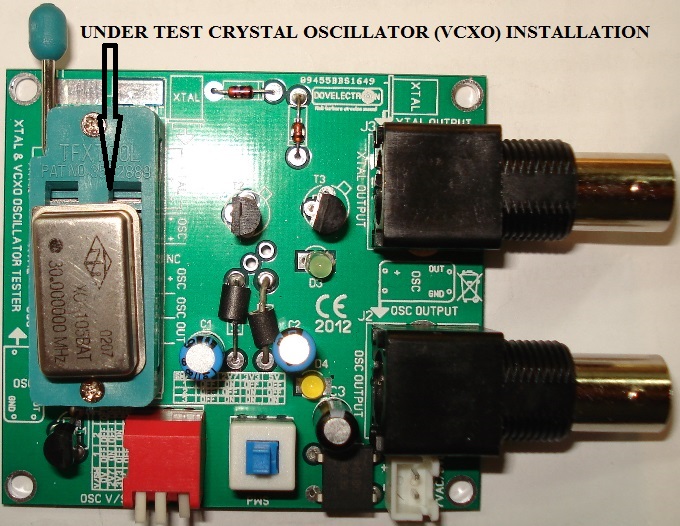
VCXO Crystal Oscillator Under Test

XTAL Under Test

SMD XTAL Test Point

Optional Outputs
BNC Female 2 Output Plugs Option A (DEFAULT)
SMA Female Jack Option B
SMA Female Jack Option C
SMA Male Jack Option D
SMA Male Jack Option E
Specifications
Xtal tester 1Mhz up to 50Mhz.
Crystal Oscillator Tester as far as it goes…(up to 250Mhz tested).
Dual Output BNC (Default) for frequency meter or oscilloscope.
Xtal Indicator Led for testing without external meters.
Power on switch & led.
A 9 V battery used as Power Supply.
5, 3.3, 2.5V Dip Switch for Different Crystall Oscillators.
Download Manual
Available In Greek
http://www.crisistech.com/blog/wp-content/uploads/2017/11/XtalGreek.pdf
Thank you.

Recent Comments